
This section describe the ArduCAM shield Rev.C hardware feature and user guide. For information about Rev.B, please refer here.
Introduction
ArduCAM shield hardware integrates all the necessary components to interface with camera modules. User only need a extra support camera modules and a TF/SD card to start image capture.
The shield provide the following features:
- Dedicate DigtalVideoPort Camera Module Interface
- Standard SPI slave bus interface
- 3.2” TFT Color LCD Screen(a)
- Build-in 3Mbit FIFO Memory
- TF/SD Card Reader with LED indicator
- Use Arduino SPI / I2C dedicate pin out
- Well mated with UNO/MEGA2560/DUE/Leonardo boards
Note: (a) Model ArduCAM-F doesn’t not include a 3.2” LCD screen
ArduCAM Shield Pin Out
ArduCAM shield includes to sets of pin out see Figure 1, they are identical in function. One is Arduino standard, it can be well mate with standard Arduino boards like UNO, MEGA2560, Leonardo and DUE etc. The other one is alternative port which can be connect to any platform like Raspberry Pi. The detail pin out for each see Table 1 and Table 2.
Figure 1 ArduCAM pin out
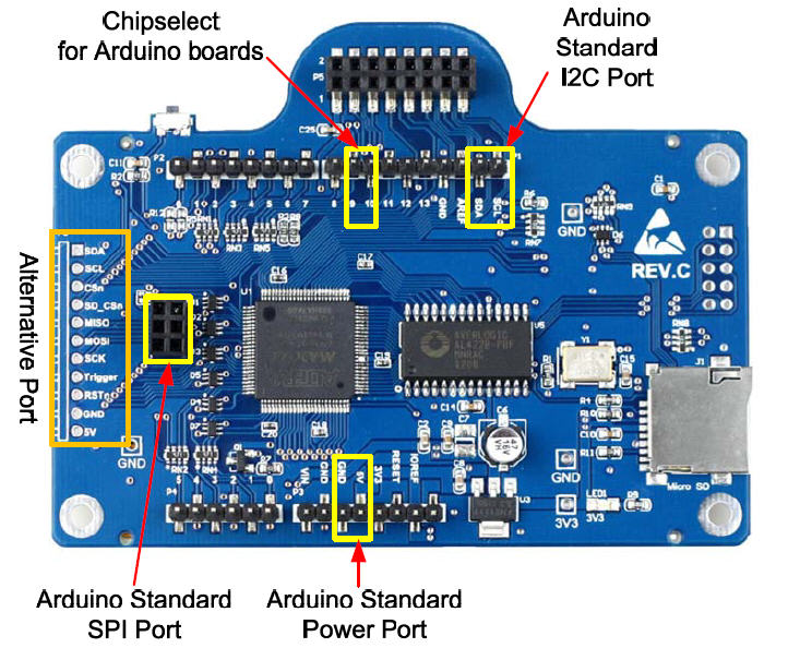
Table 1 Arduino Standard Pin Out
| Index | Arduino Pins | Description |
| 1 | I2C_SCL | I2C clock |
| 2 | I2C_SDA | I2C data |
| 3 | SPI_SCLK | SPI clock |
| 4 | SPI_MISO | SPI Master In Slave Out |
| 5 | SPI_MOSI | SPI Master Out Slave In |
| 6 | 9 | SD/TF Card Chipselect |
| 7 | 10 | ArduCAM Shield Chipselect |
| 8 | Reset | Arduino Reset Input |
| 9 | 5V | 5V Power Input |
| 10 | GND | Gound |
Table 2 Alternative Pin Out
| Index | Arduino Pins | Description |
| 1 | I2C_SDA | I2C data |
| 2 | I2C_SCL | I2C clock |
| 3 | CS_n | ArduCAM Shield Chipselect |
| 4 | SD_CSn | SD/TF Card Chipselect |
| 5 | SPI_MISO | SPI Master In Slave Out |
| 6 | SPI_MOSI | SPI Master Out Slave In |
| 7 | SPI_SCLK | SPI clock |
| 8 | Trigger | Snapshot Input |
| 9 | RST | Reset Input |
| 10 | GND | Gound |
| 11 | 5V | 5V Power Input |
Camera Interface
CMOS image sensor interfaces are divided into two categories, one is DVP (Digital Video Port) interface, the other is MIPI Mobile Industry Processor Interface. The main difference between DVP and MIPI is that DVP is a parallel interface and the MIPI interface is a high-speed differential serial interface. MIPI interface provides higher data bandwidth than the DVP interface and supports higher resolution and frame rate. Because of the complexity and need for additional hardware of the MIPI interface, we only discuss the DVP interface here.
For a standard DVP image sensor you will find the following signals:
- SCL: I2C compatible clock signal for sensor registers configuration
- SDA: I2C compatible data signal for sensor registers configuration
- XCLK: clock input to the sensor
- PCLK: clock output from the sensor,
- HREF: Line valid signal
- VSYNC: Frame valid signal
- Data[N-1..0]: Data output from the sensor, N is the internal ADC bit width.
ArduCAM shield provide a DVP interface which support wide range of camera modules from 0.3MP to 5MP. The camera modules should line up with the shield based on Pin1 shown in the Figure 2 and Table 3 provide camera interface pin out on the shield.
Figure 2

Table 3 Camera Interface Pin Out
| Pin | Signal | Pin | Signal |
| 1 | +3.3V | 2 | GND |
| 3 | SCL | 4 | SDA |
| 5 | VSYNC | 6 | HREF |
| 7 | PCLK | 8 | XCLK |
| 9 | D7 | 10 | D6 |
| 11 | D5 | 12 | D4 |
| 13 | D3 | 14 | D2 |
| 15 | D1 | 16 | D0 |
ArduChip
The ArduCAM shield includes an ArduChip which handle complex timing between MCU and LCD, Camera, FIFO. It exports a standard SPI serial interface shown in Table 4 and can be interfaced with wide range of micro-controller. MCU control the shield through a set of ArduChip internal registers shown in Table 6.
Table 4 ArduCAM shield SPI Interface
| Signal | Arduino UNO Pin | Description |
| SCL | I2C_SCL | I2C clock |
| SDA | I2C_SDA | I2C data |
| SCLK | SPI_SCLK | SPI clock |
| MISO | SPI_MISO | SPI master in slave out |
| MOSI | SPI_MOSI | SPI master out slave in |
| CSn | 10 | ArduCAM shield chipselect, active LOW |
| SD_CSn | 9 | TF/SD card chipselect, active LOW |
Bus Timing and Protocol
ArduCAM shield Rev.C use standard SPI slave bus protocol (CPOL = 0, CPHA = 0). One bus transaction composed by two 8bit access. Every bus transaction start with CSn goes low. The first 8bit is command phase, and the second 8bit is data phase. The bus timing shown in Figure 3 and Figure 4.
Figure 3 Bus Write Timing
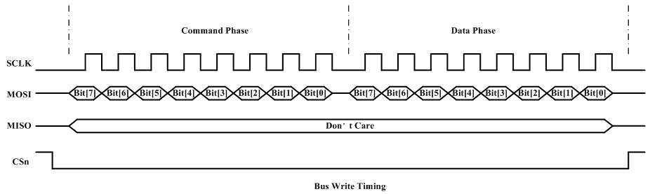
Figure 3 Bus Read Timing
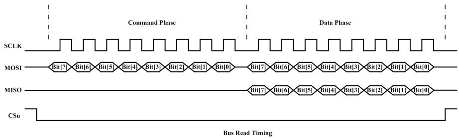
Data protocol in the command phase see Table 5
Table 5 Command Byte Protocol
Command Byte Protocol | ||||
| Bits | Bit[7] | Bit[6] | Bit[5:1] | Bit[0] |
| ArduChip Internal Register | 1: Write0: Read | 0: R/W Register1: RO Register | Register Address bit[5:1] | Register Address bit[0] |
| LCD Command Write | 1 | 0 | 11111 | 1 |
| LCD Data Write | 1 | 0 | 11111 | 0 |
| FIFO Read | 0 | 0 | 11110 | 1 |
Table 6 ArduChip Registers
| Address | Name | Mode | Description |
| 0x00 | ARDUCHIP_TEST1 | R/W | Testing Register, only used in bus testing |
| 0x01 | ARDUCHIP_TEST2 | R/W | Testing Register, only used in bus testing |
| 0x02 | ARDUCHIP_MODE | R/W | Bus Mode selection .Bit[7:3]: Reserved Bit[2]: LCD to MCU, Bit[1]: Camera to LCD , Bit[0]: MCU to LCD |
| 0x03 | ARDUCHIP_TIM | R/W | Timing Control register. Bit[7..6]: Reserved. Bit[5]: FIFO power down, 1 = power down, 0 = normal operation. Bit[4]: reserved. Bit[3]: Camera data delay control. 1 = delay 1 clock, 0 = no delay. Bit[2]: LCD backlight control, 1 = backlight off, 0 = ON. Bit[1]: Camera VSYNC polarity control, 1 = Inverted, 0 = Normal. Bit[0]: Camera HREF polarity control, 1 = Inverted, 0 = Normal. |
| 0x04 | ARDUCHIP_FIFO | R/W | FIFO control Bit[1]: Write 1 to start a capture, Bit[0]: Reset the FIFO read and write pointer to ZERO. |
| 0x40 | ARDUCHIP_REV | RO | Bit[7:6]: Revision integer part. Bit[5:0]: Revision decimal part. Default value is 0xC0. |
| 0x41 | ARDUCHIP_TRIG | RO | Trigger input Register. Bit[7:4]: Reserved. Bit[3]: Capture complete flag, 1 = Complete, 0 = Busy. Bit[2]: Reserved. Bit[1]: Capture button status, 0 = pressed, 1 = released. Bit[0]: Frame start signal, equal to VSYNC |

