This section describe the hardware feature and user guide for ArduCAM shield Rev.B. If you use later version ArduCAM shield please read the latest hardware user guide.
ArduCAM shield hardware integrates all the necessary components to interface with camera modules. User only need a extra support camera modules and a TF/SD card to start image capture.
The shield provide the following features:
- Dedicate DigtalVideoPort Camera Module Interface
- 3.2” TFT Color LCD Screen(a)
- Build-in 3Mbit FIFO Memory
- TF/SD Card Reader with LED indicator
- 6 Input/Output Software Programmable GPIOs expander
- 4 Pin Headers which well mated with UNO board


Note: (a) Model ArduCAM-F doesn’t not include a 3.2” LCD screen
Camera Interface
CMOS image sensor interface divided into two catalogs, one is DVPDigitalVideoPort interface, the other is MIPI Mobile Industry Processor Interface. The main difference between DVP and MIPI is that DVP is parallel interface and the MIPI interface is high speed differential serial interface. MIPI interface provide higher data band width than DVP interface and support higher resolution and frame rate. Because the complexity and need additional hardware of MIPI interface, we only discuss DVP interface here.
For a standard DVP image sensor you will find the following signals:
- SCL: I2C compatible clock signal for sensor registers configuration
- SDA: I2C compatible data signal for sensor registers configuration
- XCLK: clock input to the sensor
- PCLK: clock output from the sensor,
- HREF: Line valid signal
- VSYNC: Frame valid signal
- Data[N-1..0]: Data output from the sensor, N is the internal ADC bit width.
ArduCAM shield provide a DVP interface which support wide range of camera modules from 0.3MP to 5MP. The camera modules should line up with the shield based on Pin1 shown in the Figure 1 and Table 1 provide camera interface pin out on the shield.
Figure 1
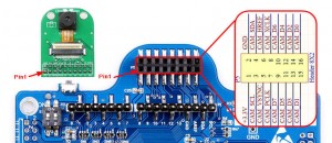

- CAM Pin Out

Table 1 Camera Interface Pin Out
| Pin | Signal | Pin | Signal |
| 1 | +3.3V | 2 | GND |
| 3 | SCL | 4 | SDA |
| 5 | VSYNC | 6 | HREF |
| 7 | PCLK | 8 | XCLK |
| 9 | D7 | 10 | D6 |
| 11 | D5 | 12 | D4 |
| 13 | D3 | 14 | D2 |
| 15 | D1 | 16 | D0 |
ArduChip
The ArduCAM shield includes a ArduChip which handle complex timing between MCU and LCD, Camera, FIFO. It exports a standard 8051 parallel interface shown in Table 2 and can be interfaced with wide range of micro-controller. MCU control the shield through a set of ArduChip internal registers shown in Table 3.
Table 2 ArduCAM shield Parallel Interface
| Signal | Arduino UNO Pin | Description |
| RS | A2 | LCD command/data selection |
| WR | A1 | Write signal shared with LCD or FIFO |
| RD | A0 | Read signal shared with LCD or FIFO |
| FIFO_CS | A3 | FIFO Chipselect |
| LCD_CS | 10 | LCD Chipselect |
| Data[0] | 0 | Data bus shared with LCD and FIFO |
| Data[1] | 1 | Data bus shared with LCD and FIFO |
| Data[2] | 2 | Data bus shared with LCD and FIFO |
| Data[3] | 3 | Data bus shared with LCD and FIFO |
| Data[4] | 4 | Data bus shared with LCD and FIFO |
| Data[5] | 5 | Data bus shared with LCD and FIFO |
| Data[6] | 6 | Data bus shared with LCD and FIFO |
| Data[7] | 7 | Data bus shared with LCD and FIFO |
Table 3 ArduChip Registers
| Address | Name | Mode | Description |
| 0x00 | ARDUCHIP_DDR | R/W | Data Direction RegisterBit[7:6]: ReservedBit[5]: IO5 input/output selectionBit[4]: IO4 input/output selectionBit[3]: IO3 input/output selectionBit[2]: IO2 input/output selectionBit[1]: IO1 input/output selectionBit[0]: IO0 input/output selection1 = output, 0 = input |
| 0x01 | ARDUCHIP_PORT | R/W | OutputPort RegisterThe value will reflect on the Pin IO0~IO6 correspondinglyBit[7:6]: ReservedBit[5]: IO5 output valueBit[4]: IO4 output valueBit[3]: IO3 output valueBit[2]: IO2 output valueBit[1]: IO1 output valueBit[0]: IO0 output value 1 = High, 0 = Low |
| 0x03 | ARDUCHIP_MODE | R/W | Bus ModeDetermine who is owner of the data bus, only one owner is allowed.Bit[7:3]: ReservedBit[2]: MCU read LCD busBit[1]: Camera write LCD busBit[0]: MCU write LCD bus |
| 0x04 | ARDUCHIP_FIFO | R/W | FIFO controlBit[1]: Write 1 to start a captureBit[0]: Reset the FIFO read and write pointer to ZERO. |
| 0x80 | ARDUCHIP_PIN | RO | Input Pin RegisterThe value will reflect the IO0~IO6 Pin status correspondinglyBit[7:6]: ReservedBit[5]: IO5 input valueBit[4]: IO4 input valueBit[3]: IO3 input valueBit[2]: IO2 input valueBit[1]: IO1 input valueBit[0]: IO0 input value 1 = High, 0 = Low |
| 0x81 | ARDUCHIP_TRIG | RO | Trigger input RegisterBit[7:4]: ReservedBit[3]: Capture complete flag, 1 = Complete, 0 = BusyBit[2]: ReservedBit[1]: Capture button status, 0 = pressed, 1 = releasedBit[0]: Frame start signal, equal to VSYNC |
| 0x82 | ARDUCHIP_REV | RO | Bit[7:6]: Revision integer partBit[5:0]: Revision decimal partFirst revision released ID is 0x40, means V1.00 |