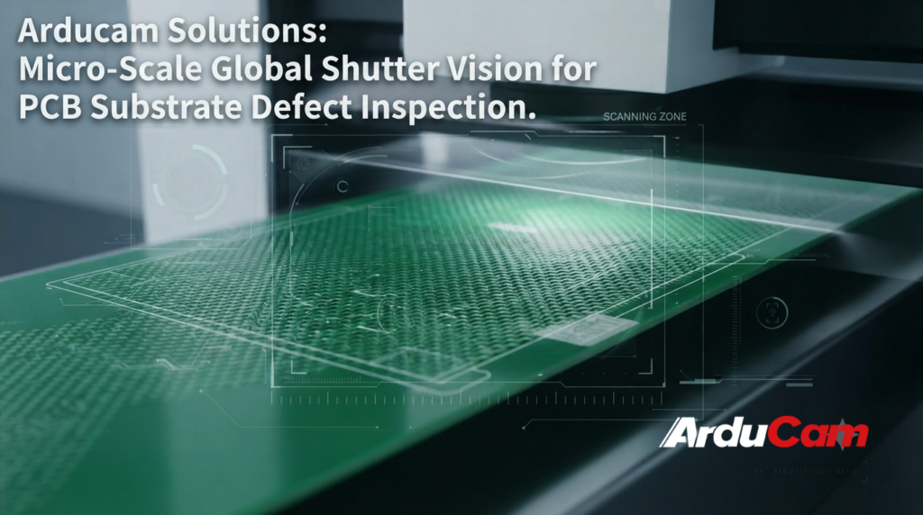
In the fast-paced world of electronics manufacturing, the reliability of printed circuit boards (PCBs) begins at the very foundation: the base materials. Inspecting raw core substrates—specifically the delicate interface between epoxy resin layers and woven glass cloth (electronic fabric)—is one of the most demanding tasks in machine vision. Microscopic flaws like pinholes, micro-cracks, resin voids, or glass weave exposed defects can compromise an entire batch of electronics if left undetected.
Recently, Arducam partnered with a well-known manufacturing leader whose existing visual inspection system was struggling to deliver reliable results on these complex, semi-transparent PCB base materials. Through close communication, deep technical collaboration, and flexible hardware adaptation, Arducam delivered a tailored solution utilizing our advanced Global Shutter Camera Series, transforming their quality control capabilities.
1. The Inspection Bottleneck: Why PCB Defect Detection Fails Traditional Systems
Inspecting PCB substrate layers introduces unique physical and optical hurdles that conventional machine vision systems simply cannot clear:
- Complex Material Backgrounds & Low Contrast: Electronic cloth is woven from glass fibers and impregnated with epoxy resin, resulting in a complex, semi-transparent grid texture. Distinguishing between normal, intricate fiber textures and true micro-defects often yields extremely low contrast, leading to high false-alarm rates.
- Microscopic Defect Tolerances: Flaws in the resin layer or embedded weave are typically microscopic in scale. Without pixel-level optical sharpness and precise resolution, inspection systems easily miss critical defects.
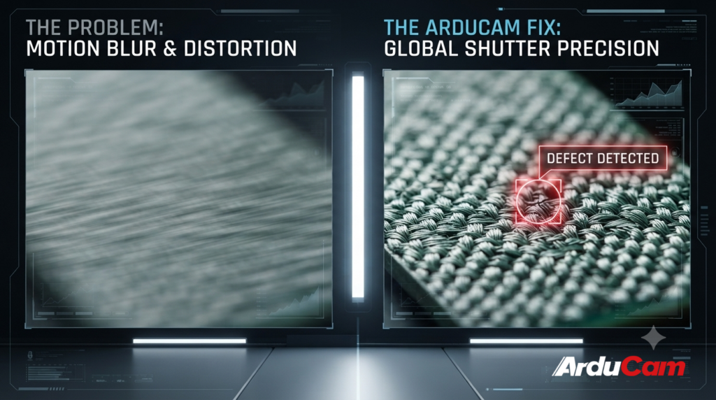
- High-Speed Material Flow: Substrate inspection lines operate under continuous, high-speed motion. Standard cameras suffer from motion blur or rolling shutter distortion, obscuring vital surface details.
- Rigid Space and Hardware Limitations: Custom inspection machinery has tight internal footprints, while different production lines demand varying line speeds, optical lenses, and interface setups.
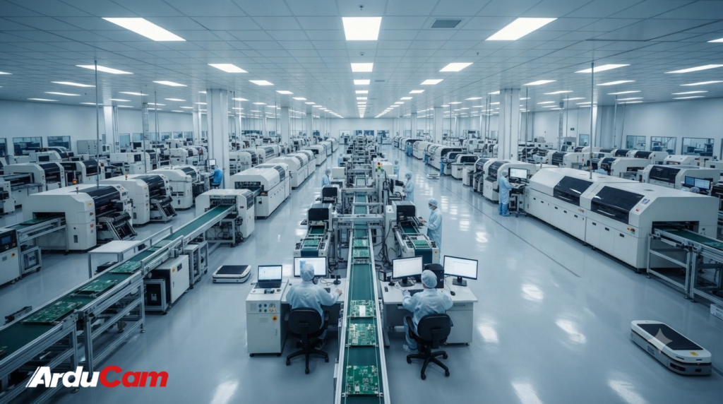
2. Collaborative Engineering: The Arducam Custom Solution
Solving these complex substrate inspection challenges required more than generic off-the-shelf components. Through continuous, iterative collaboration with the client’s engineering team, Arducam deployed a precision-engineered solution:
- Global Shutter Precision & Sharp Image “Feed”: We integrated specialized global shutter cameras to completely eliminate rolling shutter skew and motion blur. By capturing razor-sharp, distortion-free images of fast-moving substrate webs, our cameras provide high-purity, artifact-free visual “feed” that allows backend algorithms to accurately separate normal texture from actual defects.
- Customized Hardware Adaptation: To solve the client’s spatial constraints and diverse optical requirements, Arducam leveraged its flexible ecosystem to customize form factors, optimize sensor layouts, and tailor interface integrations.
- Deep Collaborative Partnership: Through routine technical syncs and close communication, Arducam worked side-by-side with the client to fine-tune exposure control, multi-camera synchronization, and illumination matching for semi-transparent composite materials.
3. Realized Impact: Elevating Precision and Production Confidence
The implementation of Arducam’s global shutter custom solution delivered an immediate leap forward in the client’s manufacturing line performance:
- Eliminated False Positives & Missed Defects: By providing ultra-sharp, high-contrast imagery of the epoxy resin and glass cloth matrix, the system accurately isolates microscopic flaws without getting tricked by complex underlying textures.
- Seamless Line Integration: The compact, customized camera hardware fit effortlessly into the client’s existing optical inspection housing, avoiding costly structural redesigns.
- Future-Proof Scalability: The success of this project established a robust, adaptable vision foundation, empowering the manufacturer to deploy consistent, high-reliability inspection across multiple production lines.
4. Product Spotlight: Arducam Industrial Global Shutter Series
The core driver behind this successful PCB substrate inspection upgrade is Arducam’s specialized Global Shutter Camera Series, engineered specifically for high-speed, micro-precision industrial measurements.
Key Technical Advantages:
- True Global Shutter Architecture: Exposes all pixels simultaneously to completely eradicate motion blur on high-speed moving webs or conveyor lines.
- Exceptional Image Purity: Captures high-contrast details on challenging surfaces, such as semi-transparent, reflective, or complex textured materials.
- Flexible Customization & Integration: Designed to adapt smoothly to diverse optical layouts, specialized lenses, and tight industrial enclosure constraints.
Looking to overcome complex material inspection hurdles and elevate your PCB or surface defect detection accuracy? 👉 Visit our Global Shutter Camera WIKI Page to explore our modular options, or reach out to our engineering team to start your custom solution collaboration.